 |
| |
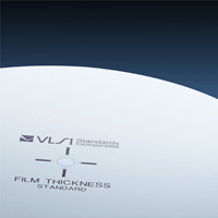 |
| Pictured is a 300 mm Silicon Dioxide Thin Film Thickness Standard. The certified area encircled at its center, is an ample 10 mm in diameter. |
NOURISH YOUR THIN FILM THICKNESS MEASUREMENT STANDARDS. Use the Thin Film Thickness Standard (FTS) to verify the accuracy of single wavelength or spectroscopic ellipsometers (SWE or SE) and reflectometers. The thin film thickness measurement standards also allow you to monitor long term tool stability in support of ISO and TS accreditation programs, and eliminate the unwanted effects of airborne molecular contamination (AMC) on your measurements.
Silicon Dioxide Film Thickness Standards (FTS) Product Description
The Thin Film Thickness Standard from VLSI Standards consists of a silicon wafer that has a pattern of uniform, thermally grown silicon dioxide on the polished surface. The silicon wafer meets all SEMI Standard specifications according to M1 - 9X for Polished Monocrystalline Silicon Wafers. The certified area of the thin film thickness measurement standard is enclosed in a 10 mm diameter, patterned region at the center of the wafer. Available wafer sizes include 100 mm, 125 mm, 150 mm, 200 mm and 300 mm.
The certified and traceable measurand is the calculated thin film thickness standard for fixed index of refraction 1.46. The derived thin film thickness measurement standard value is determined using a single layer model, with the refractive index of the silicon substrate chosen to match the values used by the National Institute of Standards and Technology.
Silicon Dioxide Film Thickness Standards (FTS) Product Specifications
- SEMI Specification Silicon Wafers
100, 125, 150, 200 and 300 mm diameter wafers
- Available Silicon Dioxide Thicknesses
2, 4.5, 7.5, 12, 25, 50, 100, 200, 400, 675, and 1010 nm.
- Traceability
SI Units through NIST

|