 |
| |
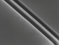 |
| Above is an isometric view of a NanoCD 70 nm line, which extends to 3 mm total certified length. |
| |
 |
|
  |
STAY IN LINE WITH SUB-100 NM ACCURACY CALIBRATION. The NanoCD™ (NCD) is the first commercially available calibration standard to provide line width accuracy calibration at the 130 nm, 90 nm and 45 nm nodes. Use this line width accuracy calibration standard for tool matching, calibrating the line width CD-AFM tip or diagnostics in a CD-SEM, and prevent bias from ever leaving the mask shop.
NanoCD Standards (NCD) Product Description
The NanoCD calibration standard consists of a small chip containing a single isolated line 4 mm long (3 mm long), offering thousands of distinct measurement sites. Chips are fabricated at VLSI Standards using a patented technique that results in line width calibrations with high uniformity and low associated uncertainty, unachievable through conventional lithography methods. For compatibility with reticle handlers, the chip is mounted to an aluminum replica of a quartz photomask.
The width of the line, or the Critical Dimension (CD), is certified with TEM and is traceable to the international system of units (SI) through the atomic lattice spacing of single crystal silicon.
NanoCD Standards (NCD) Product Specifications
- Nominal CD Values
70 nm, or 110 nm
- Accuracy
70 nm ± 0.7 nm, 110 ± 0.8 nm
- Material of CD line
Amorphous Silicon
- Length of Line
3 mm certified
- Defectivity of Line
5% Max. (150 µm of total 3,000 µm)
- Traceability
Traceable to the SI units through the atomic lattice spacing in the silicon crystal by TEM
- SEMI Specification Silicon Wafers
200 and 300 mm diameter wafers available in X or X,Y configuration
|