 |
| |
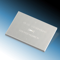 |
| The Surface Topography Standard, shown at right, consists of an etched silicon dioxide "waffle pattern" on a silicon substrate. |
STAY ON TOP OF 3D PROBE CALIBRATION. The Surface Topography Standard (STS) uses a combination of step height and pitch to enable three-dimensional surface topography calibration of optical interferometric microscopes and AFMs. Multiple pitch gratings take surface topography calibration further, allowing characterization of scan linearity. On high resolution tools such as the Atomic Force Microscope, traceable calibration can be achieved, driving your equipment to its full potential.
Surface Topography Standards (STS) Product Description
The Surface Topography Standard consists of a 12 mm x 8 mm silicon die with a pitch cluster patterned in a layer of silicon dioxide. The pitch cluster contains three distinct grid patterns. Each grid pattern measures approximately 270 µm x 270 µm and consists of an array of alternating bars and spaces with an extremely uniform pitch in both the X and Y direction. Two models are available: the Surface Topography Standard 2 has pitches of 1.8 µm, 3 µm, and 5 µm; the Surface Topography Standard 3 has pitches of 3 µm, 10 µm, and 20 µm. Each Surface Topography Standard model is available with vertical step heights of either 18 nm, 44 nm, 100 nm or 180 nm. Our precise manufacturing technique ensures a very regular topographic pattern, allowing accurate measurement across the entire working area of the standard.
Surface Topography Standards (STS) Product Specifications
- Dimensions
12 mm x 8 mm silicon die
- Materials
Silicon Dioxide on Silicon coated with Platinum (except STS2-1000S & STS2-1800S models)
- Nominal Pitch Values (X and Y)
STS2: 1.8 µm, 3 µm, and 5 µm (all on one standard)
STS3: 3 µm, 10 µm, and 20 µm (all on one standard)
- Nominal Height Values (Z)
18 nm, 44 nm, 100 nm, 180 nm
- Traceability
SI Units through NIST

|